What Anderon Actually Is — And Why It’s Structurally Unusual
Anderon is a pure-play quantum foundry — a company that exists exclusively to fabricate quantum chips for outside customers. IBM and the U.S. Department of Commerce announced the venture on May 21, 2026, via a Letter of Intent, positioning it as America’s first business of its kind. No comparable predecessor exists in the quantum industry. Every major quantum hardware company to date has manufactured chips for its own systems. Anderon breaks that pattern entirely.
The structural choice matters as much as the mission. IBM spun Anderon out rather than simply designating an internal fab division for outside work. That separation insulates the foundry from IBM’s broader commercial interests, which is a prerequisite for convincing competitors and startups to hand their most sensitive fabrication work to an IBM-affiliated entity. A hardware company running its own foundry on the side carries obvious conflicts of interest. A legally distinct spinoff carries third-party credibility that an internal unit never could.
The model IBM is replicating is TSMC’s. When TSMC launched in 1987, it decoupled semiconductor manufacturing from chip design, allowing fabless companies to develop novel architectures without building billion-dollar fabs. That separation created the conditions for the modern chip ecosystem. Anderon applies the same logic to quantum hardware: separate fabrication from design so that trapped ion startups, photonic companies, and neutral atom developers can access world-class manufacturing without funding a competitor’s roadmap. IBM retains its own quantum hardware business while Anderon operates as independent infrastructure.
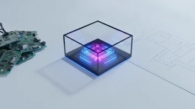
The 300mm wafer format IBM chose for Anderon reinforces that this is an industrial-scale commitment, not a research pilot. Classical chip fabs migrated to 300mm decades ago because larger wafers reduce per-chip costs dramatically. Bringing that format to superconducting quantum chips signals that Anderon is built for volume production from the start, not retrofitted from a lab environment.
The 300mm Wafer Gamble Most Reporters Are Glossing Over
IBM’s choice to build Anderon around 300mm wafer fabrication is the most consequential — and least scrutinized — technical decision buried inside the CHIPS Act quantum announcement. Most quantum hardware companies working with superconducting circuits operate on 200mm CMOS-compatible fabs, which cost less to qualify and align with existing semiconductor infrastructure. IBM is going bigger, literally.
The economics of that choice are brutal and deliberate. A 300mm fab carries substantially higher capital costs than a 200mm facility — not just in equipment, but in cleanroom construction, process qualification, and yield optimization. That premium only pencils out if you expect chip volumes to eventually approach classical semiconductor scale. IBM and the Department of Commerce are making a joint bet that quantum chip demand will get there. They are building the factory before the demand curve arrives.
That sequencing creates a specific failure mode. If adoption of fault-tolerant quantum systems stalls — whether from technical delays in error correction, slow enterprise uptake, or competing modalities like trapped ion or neutral atom pulling customers away — Anderon enters the market carrying the overhead of a large-scale fab without the throughput to justify it. Overcapacity at that cost structure doesn’t just hurt margins. It undermines the foundry model itself, because customers evaluate foundries partly on unit economics and financial stability.
The $2 billion CHIPS package spreads risk across nine companies and multiple hardware approaches, which means the federal investment is hedged even if IBM’s 300mm bet underperforms. Anderon is not hedged. It is a single-architecture, single-wafer-size operation staking its unit economics on a volume ramp that has no guaranteed timeline. The CHIPS funding reduces the near-term cash burn, but it does not restructure the underlying capacity risk. If 300mm proves five years premature, the foundry carries that weight alone.
The Government’s Dual Strategy: Centerpiece and Hedge
The $2 billion CHIPS Act quantum package announced on May 21, 2026 distributes funding across nine companies operating across trapped ion, photonic, and neutral atom platforms. That breadth is deliberate. Policymakers are refusing to declare a single quantum modality the winner before the field has produced one, keeping optionality alive across fundamentally different hardware architectures that each carry distinct advantages and failure modes.
But the funding is not evenly distributed, and the structure tells a different story than the headline diversity suggests. IBM’s Anderon foundry — spun out as America’s first pure-play quantum chip manufacturer — carries the largest and most capital-intensive commitment in the package. Anderon is built around 300mm superconducting silicon fabrication, the same wafer standard that defines leading-edge classical semiconductor production. That infrastructure choice requires massive upfront investment in tooling, cleanrooms, and process development. The government’s willingness to anchor the package around that commitment effectively designates superconducting silicon as the primary U.S. quantum technology, at least for the fabrication infrastructure cycle ahead.
The tension between these two positions — broad modality hedging and concentrated foundry investment — reflects a genuine unresolved argument inside U.S. quantum industrial policy. Building a 300mm fab takes years and locks in process assumptions before fault-tolerant quantum computing has validated any single architecture at scale. Spreading smaller bets across competing approaches preserves the ability to pivot. Doing both simultaneously means the U.S. is hedging at the research and development layer while concentrating at the manufacturing infrastructure layer.
That combination is either sophisticated strategy or an internal contradiction that will become visible when the field matures. If superconducting silicon scales toward fault tolerance first, the Anderon investment looks prescient. If a competing modality overtakes it, the foundry infrastructure becomes a stranded asset while the hedge bets remain underfunded to capitalize on the opportunity.
What a Quantum Foundry Model Changes for the Broader Ecosystem
Anderon’s pure-play model reshapes the economics of building quantum hardware from the ground up. A startup designing superconducting qubits today faces a brutal capital requirement: build your own cleanroom or license time on research-grade tools never designed for volume production. A dedicated 300mm foundry changes that equation. Quantum hardware companies could submit chip designs to Anderon the same way fabless semiconductor companies send designs to TSMC — paying for wafer runs rather than constructing fabrication infrastructure. The capital barrier to entering the superconducting qubit space drops from hundreds of millions to the cost of a design team and a purchase order.
That opportunity creates an immediate structural tension. Anderon’s business case depends on filling 300mm capacity with outside customers, but those customers are early-stage companies that may not yet have tape-out-ready designs, established process design kits to work from, or the funding to place volume orders. The foundry needs a mature ecosystem to justify its scale; the ecosystem needs the foundry to mature in the first place. IBM is betting that standing up the supply side of that equation — with CHIPS Act backing absorbing some of the demand risk — will pull customers into existence faster than waiting for organic market development.
The ripple effects extend beyond superconducting qubits. Trapped ion companies like IonQ and Quantinuum, and photonic approaches backed by firms like PsiQuantum, operate on fundamentally different fabrication requirements, but they share the same underlying problem: no dedicated quantum manufacturing infrastructure exists at scale. A well-capitalized superconducting foundry running 300mm processes widens the manufacturing maturity gap between superconducting qubits and every competing modality. Iteration cycles accelerate. Process yields improve. Cost per qubit falls. Trapped ion and photonic players now face pressure to locate or create equivalent fabrication answers — whether through dedicated partnerships with existing fabs, custom tooling investments, or their own government funding pushes — or accept a compounding disadvantage as Anderon scales production and drives down the cost curve for superconducting hardware.
The Missing Context: Is This 2004 TSMC or 1994 Sematech?
The TSMC comparison writes itself and is almost certainly wrong. When TSMC opened its doors in 1987, fabless chip designers already existed — companies with products, customers, and revenue that simply needed manufacturing capacity. TSMC plugged into a live ecosystem. Anderon is doing something structurally different: building fabrication infrastructure for an application landscape that has not yet produced a single commercially dominant quantum use case. The customers Anderon needs are not waiting in a queue. Many of them do not exist yet.
The sharper historical parallel is Sematech, the government-backed semiconductor consortium launched in 1987 with federal funding to arrest American decline in chip manufacturing. Sematech succeeded — it preserved U.S. fab capability and eventually helped close the technology gap with Japanese competitors — but it took well over a decade before those investments translated into unambiguous commercial returns. The program was a long-duration infrastructure bet, not a near-term economic catalyst.
That precedent raises the question mainstream CHIPS Act coverage keeps avoiding: if commercially meaningful quantum advantage remains five to ten years out, Anderon could be fully constructed and operational before its intended customers can absorb what it produces. A foundry without volume orders does not sit quietly. It generates operating costs, political scrutiny, and ammunition for the next congressional budget fight.
The $2 billion CHIPS quantum package is spread across nine companies, with Anderon as the centerpiece. That diversification hedges modality risk — trapped ion, photonic, and neutral atom approaches all receive smaller allocations alongside IBM’s superconducting bet. But spreading the portfolio does not resolve the timing problem. Infrastructure built five years early is not visionary. It is expensive and idle. The honest version of this story acknowledges that 2025 may be exactly the right moment to start construction, or it may be the moment the government locked in a decade of underutilization. Current evidence does not cleanly support either conclusion, and the headlines are not admitting that ambiguity exists.